The Center for Chip Design is established to promote advanced research and innovation in the field of semiconductor technology and integrated circuit design. The center provides students and researchers with opportunities to learn, design, and develop modern electronic chips used in various applications such as communication systems, embedded systems, artificial intelligence devices, and consumer electronics.
The center aims to bridge the gap between academic learning and industry requirements by providing hands-on experience in chip architecture, digital and analog circuit design, and semiconductor technologies. Through research projects, training programs, and industry collaboration, the center prepares students to meet the growing demand for skilled professionals in the semiconductor and VLSI industries.
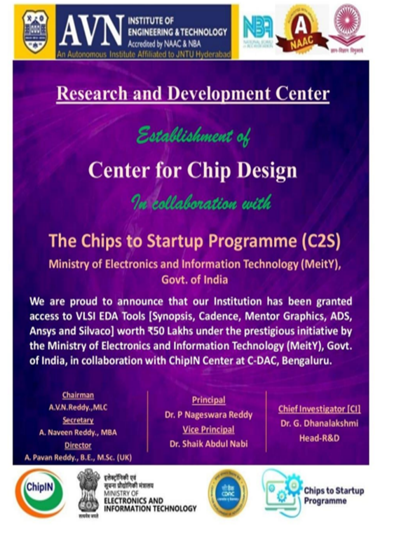
Center of Excellence (CoE) in VLSI Design and Chip Prototyping.
To leverage the access to industry-standard EDA tools under MeitY’s C2S Program, our institution is establishing a Center of Excellence (CoE) in VLSI Design and Chip Prototyping. The CoE aims to create a hub for advanced research, skill development, and innovation in semiconductor design. It will focus on core areas such as Digital and Analog IC design, RTL to GDSII flow, SoC development, and FPGA-based prototyping. Equipped with state-of-the-art tools like Cadence, Synopsys, and Mentor Graphics, the center will train students, mentor research scholars, and collaborate with industry and academia. It will also promote IP development, student internships, and project-based learning. By hosting workshops, short-term courses, and supporting academic projects, the CoE will play a crucial role in building India’s semiconductor talent pipeline. This initiative aligns with the vision of Atmanirbhar Bharat and positions our college as a contributor to the national VLSI design ecosystem.
Vision & Mission
Vision:
To be a nationally recognized hub for innovation, research, and skill development in VLSI design and semiconductor technologies, fostering industry-ready talent and contributing to India’s self-reliance in chip design.
Mission:
- To empower students and researchers with cutting-edge EDA tools and practical VLSI design knowledge.
- To promote high-quality research, IP generation, and industry collaboration.
- To create a sustainable ecosystem for semiconductor education and innovation.
Objectives:
- Provide hands-on training in digital, analog, and mixed-signal IC design using industry-grade EDA tools.
- Facilitate academic and industrial research leading to publications, patents, and IP submissions under the C2S program.
- Encourage student innovation through projects, internships, and FPGA/ASIC-based product development.
- Organize workshops, FDPs, and certificate courses in advanced VLSI topics to upskill faculty and students.
- Build strategic collaborations with other C2S institutes, startups, and semiconductor companies for joint development and knowledge sharing.
FACILITY- INFRASTRUCTURE
The Center of Excellence in VLSI Design and Chip Prototyping is equipped with advanced computing infrastructure and licensed access to industry-standard EDA tools under the MeitY C2S initiative. The lab supports the complete semiconductor design flow including Digital IC Design, Analog/Mixed-Signal Design, SoC development, FPGA prototyping, and RF simulations. With high-end Linux-based workstations, centralized license management, and support equipment, the CoE serves as a hands-on training and research platform for students, faculty, and innovators.
FACILITY- EDA Tools
- CADENCE
- SYNOPSYS
- MENTOR GRAPHICS (Siemens EDA)
- ADVANCE DESIGN SYSTEM
- ANSYS
- SILVACO
CI [Chief – Investigator]
Dr. G. Dhanalakshmi M.E, Ph.D
Head – R &D, Prof essor/ECE
Co-CI
Mr. Sharath Chandra Miryala M.Tech, (Ph.D)
Coordinator – R & D, Assistant Professor/ ECE